Executive Summary
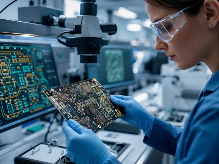
In high-precision medical electronics, the PCB stackup design is much more than a simple arrangement of layers; it is a critical component of the circuit’s electrical performance. This article explores the fundamental engineering behind layer sequencing, material physics (Dk and Df), and structural symmetry, adhering to IPC-2221 standards to guarantee long-term clinical reliability.
1. Material Science: Selecting the Right Dielectric
The foundation of a robust stackup lies in the selection of the Core and Prepreg (PP). For medical applications, we prioritize materials with a high Glass Transition Temperature (High-Tg > 170°C). The Dielectric Constant (Dk) and Dissipation Factor (Df) are the most critical parameters. A stable Dk ensures that signal velocity remains constant across different frequencies, which is vital for the high-speed data transmission found in imaging and diagnostic equipment. This material precision is a prerequisite for complex projects like 6-Layer HDI Fabrication.
2. The Physics of Symmetry: Managing CTE
Symmetry is not just an aesthetic choice; it is a mechanical necessity. During the lamination and reflow processes, materials expand and contract. If the stackup is asymmetrical—for instance, having uneven copper distribution or mismatched dielectric thicknesses relative to the center axis—the Coefficient of Thermal Expansion (CTE) mismatch will lead to permanent board warpage. At JS Circuit, our DFM Review process includes a “Balance Analysis” to ensure that copper percentages are uniform across mirror-image layers, preventing “potato-chipping” during assembly.
3. Signal Integrity through Tight Coupling
Effective stackup design utilizes Tight Coupling between signal layers and their adjacent reference planes (Ground or Power). By reducing the dielectric thickness between these layers (often using thin 1080 or 2113 Prepregs), we decrease the return path loop area. This minimizes Electromagnetic Interference (EMI) and crosstalk, which is essential for low-noise medical sensors. Layer sequencing typically follows a Signal-Ground-Signal-Power logic to ensure every high-speed trace has a dedicated, low-impedance return path.

4. Copper Weight and “Thieving”
Managing copper density is a common challenge in multi-layer boards. If a layer has large empty areas of copper, it can cause “resin starvation” during lamination, leading to internal delamination. We implement Copper Thieving—adding non-functional dots or grids of copper in low-density areas—to balance the resin flow. This ensures a uniform board thickness and consistent characteristic impedance, which we further validate during our Quality Validation & Testing phase.
FAQ: Advanced Stackup Insights
Q1: How does Dk tolerance affect my medical device?
Even a 5% variation in Dk can shift your impedance by several ohms. For high-frequency medical signals, we specify high-performance laminates with ±1% tolerance to ensure signal timing remains within strict windows.
Q2: Why avoid odd layer counts (e.g., 5 or 7 layers)?
Odd layer counts are inherently asymmetrical. They significantly increase manufacturing costs due to complex lamination cycles and almost always result in board warpage, making them unsuitable for IPC Class 3 medical standards.
Q3: What is the benefit of using “V-score” or “Tab-routing” in stackup DFM?
This relates to mechanical stress. Proper stackup design must account for the stress of singulation. We ensure ground planes are backed away from the board edge to prevent shorts during the cutting process.
Q4: Can JS Circuit help design a custom stackup from a schematic?
Absolutely. Our engineering team can generate a professional stackup proposal based on your impedance requirements, power needs, and thermal constraints, ensuring a first-pass success rate.
Optimize Your Stackup Today
Avoid signal noise and board warpage with a scientifically engineered stackup. Contact our technical team for a free consultation.