Strategic Insights: High-Density Interconnect (HDI) PCB Technology
The landscape of modern electronics is defined by an aggressive push toward miniaturization without sacrificing processing power. As consumer demand for “smart” everything scales, the internal architecture of devices has transitioned from standard through-hole designs to sophisticated HDI PCB solutions. This technology allows for a higher wiring density per unit area than conventional circuit boards, utilizing fine lines and spaces, non-mechanical microvias, and high-performance thin materials.
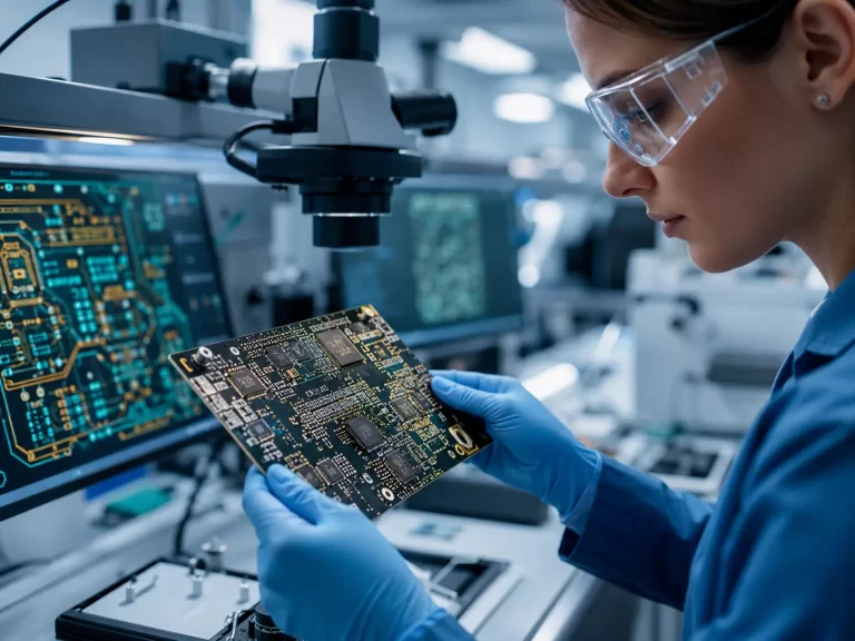
In high-stakes B2B hardware development, the decision to migrate to high-density interconnects is often a mechanical necessity. When a standard 8-layer board exceeds the physical housing of a wearable or a 5G module, engineers must leverage the sequential build-up (SBU) processes found in an any-layer HDI PCB assembly. This transition represents more than just a size reduction; it is a fundamental shift in how electrical signals are managed across the substrate.

The Technical Architecture of High-Density Interconnects
At the heart of the HDI revolution is the microvia. Unlike traditional mechanical drills that are limited by bit size and physical stress on the substrate, HDI utilizes laser-drilled microvias with aspect ratios that allow for much smaller pad diameters. This enables “Via-in-Pad” technology, where components are mounted directly over the interconnects, freeing up valuable surface real estate that was previously wasted on fan-outs.
To maintain the highest levels of quality and precision, it is vital to understand the heritage and technical capabilities of your manufacturing partner. You can learn more about us and our decades of expertise in precision lamination. A leading high-end HDI PCB factory will typically offer line and space (L/S) capabilities as fine as 30μm, combined with advanced staggered or stacked via structures that provide the shortest possible electrical paths for high-speed signals.
Technical Comparison: Standard vs. HDI Parameters
| Parameter | Standard Multilayer PCB | HDI PCB Technology | B2B Impact |
| Minimum Trace/Space | 100μm – 125μm | < 75μm (down to 30μm) | 4x higher density |
| Via Type | Through-hole (Mechanical) | Microvia (Laser-drilled) | Reduced Parasitics |
| Interconnect Density | Low – Moderate | High – Extreme | Compact form factor |
| Aspect Ratio | 8:1 – 10:1 | 0.75:1 – 1:1 | Improved Reliability |
| Component Pitch | > 0.8mm | < 0.4mm (BGA) | Supports modern SoCs |
If you are ready to optimize your board layout for maximum density, we invite you to contact us for a comprehensive DFM (Design for Manufacturing) review of your current schematics.
Space Optimization and Signal Integrity Advantages
The primary driver for choosing HDI is space. By utilizing blind and buried vias, designers can place components on both sides of the board without interfering with signal paths on internal layers. This “any-layer” capability means a standard 12-layer board can often be redesigned into an 8-layer HDI board with better performance. This is the core service offered by a top-tier HDI PCB manufacturer, helping clients reduce total system weight and volume by up to 40%.
Beyond size, signal integrity is the silent benefactor. In high-frequency applications, traditional through-holes act as antennas, introducing parasitic capacitance and inductance that can distort signals. Microvias, being significantly shorter and narrower, minimize these effects. This reduction in “stub” length is critical for 5G communication and high-speed computing, ensuring that data packets remain intact even at frequencies exceeding 10GHz.

Understanding the Fabrication Complexity
The manufacturing of an HDI board is significantly more complex than a standard board. It involves multiple lamination cycles where thin dielectric layers are bonded to the core. This is why a thorough understanding of PCB manufacturing process explained is essential for procurement teams. Each “lamination step” introduces variables in thermal expansion and registration that must be managed with extreme precision in an industrial HDI PCB factory.
A common misconception in the industry is that HDI is always more expensive. While the HDI PCB fabrication cost per square inch is higher, the total cost of the final device often decreases. By reducing the layer count and board size, you lower the cost of the raw laminate and the external device housing. Furthermore, the improved electrical performance leads to fewer field failures and lower warranty costs, significantly boosting the lifetime ROI of the product.

Critical Applications: From Automotive to Medical
The automotive industry is currently one of the fastest-growing sectors for rigid-flex HDI PCB solutions. Modern ADAS (Advanced Driver Assistance Systems) and autonomous driving sensors require massive processing power packed into the tight crevices of bumpers and side mirrors. Similarly, the medical sector relies on PCB vs PCBA expertise to create implantable devices and portable diagnostic equipment where a failure in signal integrity is not an option.
In these safety-critical environments, the design must account for “Lot Drift” and thermal fatigue. HDI microvias are inherently more resistant to thermal cycling because their smaller aspect ratios make them less prone to barrel cracking compared to deep through-holes. This makes high-density interconnect technology the preferred choice for aerospace and defense applications where equipment must survive extreme temperature fluctuations from -55°C to +125°C.
Sourcing and Decision Logic: Selecting an HDI Partner
When evaluating a potential partner for wholesale multilayer HDI boards, buyers must look beyond the quote. You should analyze their in-house laser drilling capacity, their registration accuracy (using X-ray verification), and their experience with advanced materials like Rogers or low-Dk/Df laminates. A factory that understands what is an HDI PCB and how does it differ from traditional PCBs will be able to suggest design modifications that simplify the build and lower the scrap rate.
If X → Choose Y: The HDI Decision Matrix
-
If Component Pitch < 0.5mm (BGA) → You must use HDI with Via-in-Pad.
-
If Signal Frequency > 5GHz → Transition to HDI to minimize parasitic inductance.
-
If Device Weight is a Critical KPI → Use thin-core HDI to reduce board mass.
-
If Prototype Budget is Limited → Consider a “hybrid” HDI approach (standard layers + 1 HDI layer) to balance cost and density.
Strategic Conclusion
In conclusion, the HDI PCB is no longer a niche luxury; it is the fundamental platform for the next generation of industrial and consumer hardware. Whether you are shrinking a wearable or optimizing a high-speed router, the advantages of space, weight, and signal integrity make HDI the clear winner. By partnering with a factory that provides integrated any-layer HDI PCB assembly, you ensure that your product is not only smaller but more reliable and future-proof.

FAQ
1. What makes an HDI PCB different from a standard multilayer board?
An HDI PCB utilizes microvias (typically <150μm), thinner materials, and higher trace densities than standard boards. While traditional boards use mechanical drilling to go through all layers, HDI boards use laser drilling and sequential build-up (SBU) to create blind and buried vias. This allows for significantly more compact designs and shorter signal paths, which are vital for high-speed electrical performance and miniaturized consumer electronics.
2. Why is microvia technology critical for modern electronics?
Microvias are the “veins” of high-density interconnect technology. Because they are laser-drilled and have a very low aspect ratio (typically 0.75:1), they can be placed within component pads (Via-in-Pad). This eliminates the need for large fan-out traces, allowing designers to utilize BGAs with pitches as small as 0.4mm. Furthermore, their small size reduces parasitic capacitance and inductance, which is essential for maintaining signal integrity at 5G and 6G frequencies.
3. How does HDI technology impact the total cost of a device?
While the unit cost of an HDI PCB manufacturer‘s board may be higher due to complex lamination and laser drilling, the total system cost often drops. HDI allows you to reduce the layer count (e.g., turning a 10-layer standard board into a 6-layer HDI board) and the overall board size. Smaller boards mean smaller enclosures and less material used throughout the product, often resulting in a more competitive price point for the end consumer.
4. Are HDI PCBs reliable for automotive and medical applications?
Yes, provided they are manufactured by a high-end HDI PCB factory following IPC Class 3 standards. Microvias are actually more reliable in high-vibration and thermal-shock environments than traditional through-holes because their small size makes them more flexible and less prone to stress-induced cracking in the barrel. This reliability is why they are standard in ADAS systems, MRI machines, and mission-critical aerospace hardware.
5. What are the main design challenges when moving to HDI?
The primary challenges are managing the “Any-Layer” stack-up and ensuring proper thermal dissipation. Designers must work closely with their HDI PCB manufacturer to ensure the aspect ratio of the microvias is plateable and that the materials selected can withstand multiple reflow cycles. Proper DFM (Design for Manufacturing) is essential to avoid “via-on-via” stacking issues that can lead to connectivity failures during the assembly phase.
References
-
"High-Density Interconnect Technology: Principles and Applications," Dr. Michael Pecht, Center for Advanced Life Cycle Engineering (CALCE).
-
"IPC-2226: Sectional Design Standard for High Density Interconnect (HDI) Printed Boards," IPC — Association Connecting Electronics Industries.
-
"Thermal Reliability of Microvias in High-Density Interconnects," IEEE Transactions on Components, Packaging and Manufacturing Technology.
-
"Signal Integrity in 5G Systems: The Role of HDI Fabrication," Rogers Corporation Technical Series.
-
"Sequential Build-Up (SBU) Process Flow in Advanced PCB Manufacturing," Journal of Electronic Materials.
-
"Microvia Reliability for Aerospace and Defense Electronics," NASA Goddard Space Flight Center Technical Report.
-
"The Economic Impact of Miniaturization in Consumer Electronics," Global Sourcing Council Research.
-
"Advances in Laser Drilling for High-Density Interconnects," International Society for Optics and Photonics (SPIE).
Technical Intelligence: HDI Fabrication and Strategic Decision Matrix
How does HDI technology solve miniaturization bottlenecks?
The shift to HDI PCB fabrication is primarily driven by the physical limitations of mechanical drilling. Traditional through-holes require large annular rings that consume surface real estate; in contrast, microvia PCB design uses laser ablation to create interconnects as small as 0.075mm. This allows for Via-in-Pad structures, enabling high-pin-count BGAs (0.4mm pitch) to be routed without extensive fan-outs. The result is a device that is up to 40% smaller and 30% lighter than standard multilayer alternatives.
Strategic Selection Guide (Decision Logic)
- →
Scenario: High-Speed 5G Modules. If your design exceeds 10GHz, prioritize any-layer HDI PCB assembly to minimize parasitic inductance caused by standard via stubs. - →
Scenario: Extreme Thermal Cycling. For automotive or aerospace sensors, choose a high-end HDI PCB factory capable of staggered via structures, which offer superior mechanical resistance to thermal expansion compared to stacked vias. - →
Scenario: Cost Optimization. If your bill of materials (BOM) is tight, use a hybrid HDI stack-up (mixing HDI outer layers with standard inner cores) to achieve density while controlling the HDI PCB fabrication cost.
Industry Trends & Risk Mitigation