From Routing Congestion to Breakthrough: The HDI PCB Turning Point
“Routing failed again.”
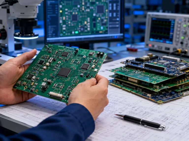
The layout engineer zoomed into the BGA escape region. 0.4 mm pitch. Differential pairs stacked. Power planes congested. Through-hole vias blocking every routing channel.
The board was only 65 × 45 mm. The product needed to shrink by another 20%.
The issue wasn’t software. It wasn’t signal speed.
It was architecture.
The turning point came when the team shifted from a conventional multilayer PCB to an HDI PCB structure.
This is not just a density upgrade. It is a structural evolution in electronic interconnect technology.
In this technical deep-dive, we analyze what defines an HDI PCB, how it fundamentally differs from traditional PCB architecture, and why modern OEMs increasingly adopt HDI strategies with advanced manufacturers like jscircuit.

The Structural Evolution: From Mechanical Drilling to Laser Precision
Traditional PCBs were engineered in an era dominated by:
-
1.0 mm BGA pitch
-
Sub-500 MHz clock speeds
-
Moderate routing density
-
4–8 layer designs
But today’s products demand:
-
0.3–0.5 mm pitch BGAs
-
Multi-GHz differential signaling
-
Compact mobile architectures
-
RF + digital hybrid layouts
An HDI PCB integrates:
-
Laser-drilled microvias (≤100 μm)
-
Blind and buried via interconnections
-
Sequential lamination cycles
-
Ultra-fine trace/space (≤75 μm)
This is not incremental improvement. It is a manufacturing paradigm shift.
According to IPC-2226 classification standards, HDI boards can achieve interconnect densities up to 3× higher than traditional multilayer PCBs.
At About jscircuit, engineering reports indicate that over 70% of high-speed and miniaturized OEM projects now require HDI stack-ups to meet space and signal integrity constraints.
Traditional PCB Limitations in Modern Systems
Through-hole vias connect all layers vertically. That sounds efficient — until routing congestion begins.
Electrical Impact of Through-Hole Vias
-
Increased via stub length
-
Higher parasitic inductance
-
Reflection points in high-speed signals
-
Impedance discontinuities
Signal integrity labs have documented:
-
Up to 20% eye diagram degradation in dense BGA escape areas
-
Increased EMI emissions due to via stub resonance
HDI microvias reduce stub length dramatically, often eliminating back-drilling requirements.
When OEM teams consult early with Contact jscircuit during layout planning, they often avoid costly respins caused by routing congestion and impedance mismatch.
Engineering Deep Dive: What Makes HDI PCB Complex?
HDI PCB manufacturing is precision-driven engineering.
1. Laser Microvia Formation
Laser drilling provides:
-
Clean via walls
-
High aspect ratio control
-
Minimal dielectric damage
-
Precise depth targeting
Microvias are typically:
-
75–100 μm diameter
-
Plated with uniform copper deposition
-
Verified via X-ray inspection
2. Sequential Lamination
Unlike standard lamination (single cycle), HDI boards undergo:
-
Core lamination
-
Microvia drilling
-
Plating
-
Additional dielectric layering
-
Repeat lamination cycles
Each cycle introduces:
-
Thermal expansion stress
-
Alignment tolerance challenges
-
Copper thickness balancing requirements
The advanced workflows outlined in PCB Manufacturing Process Explained demonstrate how process control and inspection determine yield reliability.

Data-Driven Comparison: HDI PCB vs Traditional PCB
Let’s look at measurable differences.
Routing Efficiency
-
Traditional PCB: 65–75% routing efficiency in dense BGAs
-
HDI PCB: 85–95% routing efficiency
Board Size Reduction
-
Up to 40% footprint reduction
Via Count Reduction
-
30–60% fewer through-hole vias
Signal Performance
-
15–30% improvement in signal integrity for high-speed lines
Reliability Under Thermal Cycling
-
HDI microvias show improved fatigue resistance when properly plated and designed
The HDI PCB Solutions section highlights multilayer stack-ups optimized for automotive and 5G applications, where thermal and signal performance must coexist.
Why OEM Manufacturers Are Strategically Migrating to HDI
The shift to HDI is not cosmetic — it is competitive.
Drivers Behind Industry Adoption
-
5G and mmWave hardware miniaturization
-
AI accelerator board density
-
Automotive ADAS integration
-
Wearable medical devices
-
IoT module compression
A 2023 electronics manufacturing survey revealed:
-
62% of OEMs plan to increase HDI adoption within three years
-
48% cite signal integrity improvement as primary motivation
-
37% cite product miniaturization
Design Discipline: HDI Is Not Just Smaller — It Requires Strategy
Transitioning to HDI demands advanced design planning.
Critical Design Practices
-
Early stack-up definition
-
Controlled impedance modeling
-
Microvia stacking stress analysis
-
Thermal expansion matching
-
Power integrity simulation
The resource PCB Design Fundamentals and Best Practices outlines manufacturability guidelines that prevent common HDI failure modes such as:
-
Microvia cracking
-
Resin void formation
-
Plating inconsistency
-
Layer misregistration
HDI is powerful — but only when engineered holistically.
Real-World Case Insight: Density vs Performance
In one industrial computing redesign:
-
Original board: 14-layer traditional PCB
-
Routing congestion: Severe under BGA
-
Redesign: 10-layer HDI PCB
-
Result:
-
28% footprint reduction
-
Improved signal stability
-
Reduced EMI
-
Lower assembly complexity
-
Engineering-led manufacturing at jscircuit ensured microvia reliability testing, X-ray verification, and impedance validation before mass production.
The Hidden Risk: When HDI Is Done Incorrectly
HDI PCB failures usually stem from:
-
Improper microvia plating thickness
-
Excessive aspect ratios
-
Poor lamination stress control
-
Inaccurate impedance modeling
Cracked stacked vias under thermal cycling remain a known risk in poorly controlled processes.
That is why experienced HDI manufacturing capability is not optional — it is critical.
|
|
|


FAQ: What Engineers Commonly Ask About HDI PCB
1. Is HDI PCB always better than traditional PCB?
Not always. It depends on density requirements, signal speed, and space constraints. However, for fine-pitch BGA and high-speed systems, HDI provides significant advantages.
2. Does HDI PCB increase manufacturing complexity?
Yes. It requires laser drilling, sequential lamination, advanced inspection, and tighter tolerances.
3. Can HDI PCBs handle automotive-grade environments?
Yes, when designed with correct materials and plating thickness control, they withstand -40°C to 125°C cycles.
4. Is HDI suitable for RF applications?
Absolutely. Reduced via stub and controlled impedance improve high-frequency performance.
5. When should an OEM switch to HDI architecture?
When routing congestion, signal degradation, or size limitations become barriers to performance goals.
HDI PCB Is an Architectural Decision, Not Just a Technology Upgrade
Returning to the opening scenario:
The team did shrink the board.
They improved signal integrity.
They reduced layers.
They improved manufacturability.
Not by redesigning components — but by rethinking interconnect architecture.
An HDI PCB is not simply a denser board.
It is:
-
A strategic routing solution
-
A signal integrity enhancement
-
A miniaturization enabler
-
A competitive advantage
As electronics continue evolving toward higher speeds and smaller footprints, traditional PCB architectures face physical and electrical ceilings.
HDI PCB technology breaks those ceilings.
And for OEM manufacturers seeking long-term scalability, precision engineering, and production reliability, the difference between traditional PCB and HDI PCB is no longer incremental.
It is transformational.