Key Project Overview: Next-Generation AI Backplane Engineering
The AI Compute Surge and Physical Hardware Demands
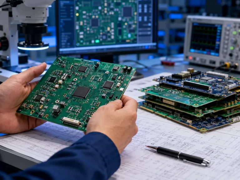
The global architecture of data processing is undergoing a paradigm shift driven by Large Language Models (LLMs) and distributed neural network training clusters. As high-density accelerators expand rapidly across hyperscale data centers, global demand for AI servers has reached unprecedented heights. This demand translates directly to a critical hardware bottleneck: the physical printed circuit board. Modern application-specific integrated circuits (ASICs) and graphics processing units (GPUs) processing compute-intensive workloads require an architecture capable of processing massive data throughput with ultra-low latency.
To support this level of data density, standard interconnect boards are no longer sufficient. Hardware architects are transitioning systems to a high-density ultra-high multilayer PCB environment. The system’s foundational core is built around a robust 20-Layer Backplane Design for AI Servers. This design serves as the primary system highway, providing seamless interconnection between compute nodes, switch fabrics, and power delivery blocks. For more engineering deep-dives, you can explore the JS Circuit Blog | PCB Manufacturing Insights, which tracks advanced structural innovations from a leading Expert PCB Supplier & Manufacturer.

The Physics of the 20-Layer Backplane Design for AI Servers
Designing a backplane that exceeds 20 layers requires balancing mechanical stability against transmission line performance. As thickness scales past 3.2mm, structural forces within the substrate can jeopardize electrical routing. Standard manufacturing lines struggle with layer registration, mechanical drill deviation, and resin contraction. This underscores the importance of choosing a highly qualified high-frequency PCB manufacturer capable of operating at tighter tolerances than standard industrial operations require.
Stackup Symmetry and Warpage Control
The primary structural challenge in high-layer count backplane manufacturing challenges is warp and bow mitigation during the thermal lamination process. A 20-layer stackup must possess absolute geometric and material symmetry relative to the horizontal center plane. If copper weights, prepreg distributions, or core thicknesses are asymmetrical, the uneven coefficient of thermal expansion (CTE) forces will bend the panel during the multi-stage pressing cycle. This balance is critical when utilizing heavy power cores alongside ultra-thin signal layers to maintain flatness across large-format panels.
To guarantee a flat profile suitable for automated surface mount technology (SMT) component assembly, the panel’s mechanical balance must be optimized during stackup definition. Standard industrial panels allow a maximum warpage of 0.75%, but an enterprise AI backplane demands a threshold below 0.50% to protect large-die silicon sockets from structural stress cracks during thermal cycling.
Power Distribution Network PDN Impedance Requirements
Modern accelerator clusters require operating currents that exceed 1000A at core voltages below 1.0V. Consequently, the power distribution network (PDN) of the 20-layer backplane must maintain extremely low target impedance across a wide frequency spectrum (from DC up to several GHz). This requires allocating multiple dedicated internal planes with thick copper layers (typically 2 oz or 3 oz) sandwiched between thin, high-capacitance dielectric cores.
These power-ground plane pairs must be placed as close to each other as fabrication limits allow. This proximity increases plane-to-plane capacitance and minimizes loop inductance, which suppresses high-frequency power rail ripple. Additionally, the spatial distribution of through-hole power vias must be optimized to prevent localized current crowding, which can create dangerous thermal hot spots exceeding the glass transition temperature of the surrounding resin matrix.
Low-Loss Material Selection for High-Speed Digital Architecture
At ultra-high data frequencies, traditional FR-4 materials act as attenuators rather than insulators. For data running at PCIe Gen 6 or 112 Gbps PAM4 signaling rates, selecting proper high-performance laminates is crucial. Engineering teams evaluating a wholesale high-speed backplane custom provider must carefully verify dielectric properties across multiple operating frequencies to ensure the material remains performant under demanding workloads.
Dielectric Constant Dk and Dissipation Factor Df Mechanics
Effective low-loss material selection for high-speed digital systems requires managing two fundamental properties: the Dielectric Constant (Dk) and the Dissipation Factor (Df). Dk governs the signal propagation velocity along the transmission line, while Df dictates the amount of electromagnetic energy lost as heat within the dielectric substrate. For high-speed digital backplanes, materials with flat Dk and ultra-low Df behavior across a 1 GHz to 50 GHz span are necessary to minimize signal attenuation and phase distortion.
| Laminate Class | Typical Dk (at 10 GHz) | Typical Df (at 10 GHz) | Thermal Conductivity (W/mK) | Primary AI Server Application |
|---|---|---|---|---|
| Standard Mid-Loss | 4.20 – 4.40 | 0.0150 – 0.0200 | 0.35 | Legacy Interconnects & Basic Management Boards |
| Low Loss (Very Low Loss) | 3.60 – 3.80 | 0.0050 – 0.0080 | 0.48 | Standard PCIe Gen 5 Storage & Interconnect Matrices |
| Ultra-Low Loss (Megtron 6 Equivalent) | 3.40 – 3.50 | 0.0020 – 0.0038 | 0.55 | 112 Gbps Clustering Fabrics & OAM/UBB Boards |
| Hyper-Low Loss (Megtron 8 / PTFE Blend) | 3.00 – 3.20 | 0.0010 – 0.0015 | 0.65 | Next-Gen 224 Gbps Switches & Liquid Cooled Clusters |
Resin Systems and Glass Weave Variations
Beyond broad parameters, the micro-architecture of the glass cloth plays a major role in signal propagation. Standard E-glass weaves exhibit significant resin-rich versus glass-rich variance, which introduces timing delays (skew) between differential signal trace pairs. Advanced systems require specifying spread glass or flat glass configurations (such as 1067 or 1078 weaves) coupled with high-grade polyphenylene ether (PPE) resin chemistry.
Furthermore, standard copper foil profiles feature macroscopic roughness that forces high-frequency currents to travel longer paths due to the skin effect. Advanced designs require specifying Very Low Profile (VLP) or Hyper Low Profile (HVLP) copper foils. These smooth copper treatment options minimize skin effect resistive loss and preserve signal integrity along long backplane traces.
Advanced Interconnects: Blind and Buried Via Technology Fabrication
Routing thousands of high-speed digital nets through a 20-layer stackup requires complex vertical interconnect structures. This routing density can be achieved by transitioning from traditional through-hole vias to sophisticated blind and buried via technology fabrication methods. This shift allows engineers to reclaim routing space on critical internal signal layers.
Aspect Ratio Limitations in Ultra-High Multilayer Architectures
The aspect ratio—the ratio of board thickness to drill hole diameter—determines the plating capability of a multilayer backplane PCB factory. For a thick 20-layer board, mechanical drills face challenges when drilling through-holes below 10 mils, as drill bits break easily and chemistry can struggle to properly plate the deep copper barrel. Laser micro-vias offer an alternative, but are restricted to shallow penetration depths, typically spanning only one or two dielectric layers. Consequently, modern high-layer architectures utilize sequentially laminated substructures featuring buried vias that connect internal layer segments independently.
Via Stub Mitigation and Backdrilling Precision
When high-speed signals transfer from an upper layer to an internal layer through a long vertical via, the remaining unused portion of the via barrel forms a resonant stub. This via stub acts as an open-ended transmission line that reflects energy back down the trace, introducing deep nulls in the insertion loss profile. To eliminate this issue, engineers use advanced backdrilling techniques.
Backdrilling uses a larger mechanical drill bit to remove the unused copper stub down to a precise depth, leaving a remaining stub length below 2 mils. This requires tight depth-control tolerance from the factory’s CNC machinery, as over-drilling can destroy the internal pad connection, while under-drilling leaves behind an inductive stub that degrades signal integrity at 112 Gbps operating rates.
Signal Integrity Simulation and Electromagnetic Modeling
Hardware teams cannot rely on basic design rules for 20-layer backplane layouts; full 3D electromagnetic field solver modeling is mandatory. These simulations help predict the complex interactions of transmission lines, via transitions, and breakout regions before starting production. This reduces the risk of expensive redesign cycles and helps manage overall AI server backplane cost metrics.
Combating Insertion Loss and Crosstalk at 112 Gbps PAM4
Transitioning from NRZ encoding to PAM4 multilevel signaling reduces the required Nyquist frequency but tightens the allowed signal-to-noise ratio (SNR). Insertion loss becomes the primary concern for long routing runs across large-format backplanes. S-parameter analysis via simulation tools evaluates loss profiles across the entire layout.
Additionally, crosstalk between adjacent signal lines increases rapidly at high layer densities. To minimize both near-end crosstalk (NEXT) and far-end crosstalk (FEXT), routing configurations must use a robust ground coplanar waveguide layout or maximize line-to-line spacing. Engineers follow a strict 3H rule, where the spacing between differential trace pairs must equal at least three times the distance to the nearest reference plane layer.
Fiber Weave Effect Mitigation Strategies
As trace routing crosses alternating glass bundles and resin pockets within the substrate material, differences in localized dielectric properties alter trace impedance. This structural imbalance introduces phase skew within differential pairs. To mitigate this fiber weave effect, simulation models often recommend routing traces at a slight angular offset relative to the weave axis (typically a 5-degree to 10-degree zig-zag orientation).
Alternatively, hardware designs can specify dual-ply glass weaves or choose high-cost glass substrates with matched glass-resin dielectric properties. These mechanical and material adjustments ensure that signal propagation remains synchronous across both legs of a differential pair, preserving system eye margins at higher frequencies.
Global Compliance, Thermal Mandates, and Industry Trends
High-layer backplanes must meet global regulatory and mechanical standards before installation in commercial infrastructure. Materials must achieve a UL 94 V-0 flame-retardant rating to safeguard data centers against thermal runaway events. Additionally, compliance with European Union RoHS and REACH regulations is mandatory, prohibiting the use of specific hazardous materials in the underlying chemical matrix.
The latest industry trends focus on integrating liquid cooling loops into high-density server configurations. Direct-to-chip cooling systems can expose the surrounding circuit board to localized condensation risks and sustained thermal gradients. Consequently, backend manufacturing processes must apply moisture-resistant conformal coatings and specify moisture-resistant resin systems to protect internal layer tracking from electrochemical migration risks over long operating lifetimes.
Strategic Insights & AI-Driven Industry Analysis
Industrial Perspectives on 20-Layer Infrastructure
How Accelerated Computing Changes Hardware Design: Traditional backplane designs focused primarily on simple point-to-point connections with basic impedance targets. The emergence of high-density AI clusters changes these requirements by introducing extreme thermal loads alongside ultra-high transmission speeds. Backplanes must now operate as active shielding structures that manage high power distribution alongside low-voltage signal lanes.
Why Ultra-Low Loss Laminate Materials Are Necessary: At high operating frequencies, signal attenuation increases rapidly. Choosing a hyper-low-loss substrate like Megtron 8 or an equivalent PTFE blend is necessary to maintain clean signal eyes across long traces. While these premium materials impact initial fabrication budgets, they prevent system packet drops and minimize total power draw by reducing the need for active re-timer chips across the board layout.
Long-Term Considerations for Enterprise Hardware Deployment: When scaling production to high volumes, engineering groups must partner with factories that use automated statistical process control for high-precision backdrilling and automated optical layer alignment. Ensuring strict process control across all vertical interconnect channels is the most reliable strategy for achieving high production yields and avoiding field failures in mission-critical processing centers.
Frequently Asked Questions
1. What are the main fabrication bottlenecks when executing a 20-Layer Backplane Design for AI Servers?
The primary bottlenecks center around internal layer registration tolerances, vertical drilling accuracy, and managing mechanical warpage across thick profiles. As the layer count increases, minor deviations during the multi-stage lamination press cycle can misalign internal routing pads, leading to inner-layer shorts or open circuits that lower production yields.
2. Why is low-loss material selection for high-speed digital systems critical for AI cluster infrastructure?
High-speed signaling protocols like PCIe Gen 6 and 112 Gbps PAM4 have strict channel insertion loss budgets. Standard glass substrates attenuate signals over short distances, transforming high-frequency energy into heat. Specifying ultra-low-loss materials preserves signal eye amplitude and eliminates the need for power-hungry active signal boosters across long backplane routes.
3. How does blind and buried via technology fabrication save routing space in complex layouts?
Traditional through-hole vias penetrate the entire thickness of the board, consuming valuable routing channels on every single layer. Blind and buried vias restrict vertical transitions to specific inner or outer layer subsets, freeing up layout space on adjacent layers to support the dense routing matrices required by high-speed server clusters.
4. What specific challenges does backdrilling solve in thick, high-layer count boards?
Backdrilling removes the unused copper portion (stub) of a through-hole via after a signal transitions to an internal layer. Unremoved stubs create electrical reflections that introduce resonant nulls into the insertion loss profile, which can disrupt high-frequency data streams if not properly remediated down to a minimal length.
5. How can engineering teams mitigate the fiber weave effect across long backplane traces?
Teams can address this issue by routing high-speed differential signal traces at a slight angular offset (e.g., 5 to 10 degrees) relative to the underlying glass fabric weave. Alternatively, specifying uniform spread-glass cloth fabrics or choosing matched-dielectric resin options helps maintain uniform signal propagation velocity across both lines of a differential pair.
References
- IPC-2222B: Sectional Design Standard for Rigid Organic Printed Boards, IPC International Standard (2021).
- IEEE Transactions on Components, Packaging and Manufacturing Technology: Power Distribution Network Impedance Optimization Strategies.
- Panasonic Corporation: High-Speed Low-Loss Megtron Laminate Technical Material Characterization Reports.
- Intel Corporation: High-Speed Board Design Guidelines for Next-Generation PCIe Architectures.
- DesignCon Technical Proceedings: Mitigation Strategies for 112 Gbps PAM4 Via Stub Resonances.
- UL 94: Standard for Tests for Flammability of Plastic Materials for Parts in Devices and Appliances.
- EU RoHS Directive 2011/65/EU: Restrictions on Hazardous Substances in Multilayer Electronic Assemblies.
- Journal of Signal Integrity: Fiber Weave Induced Skew Modeling and Practical Physical Board Routing Solutions.