Tracing Failure Back to the Process
“Why did this board fail thermal cycling at 300 hours?”
The quality engineer stared at the cross-section under the microscope.
“The copper thickness variance is too high,” someone replied. “And the lamination pressure profile looks unstable.”
A silence filled the lab.
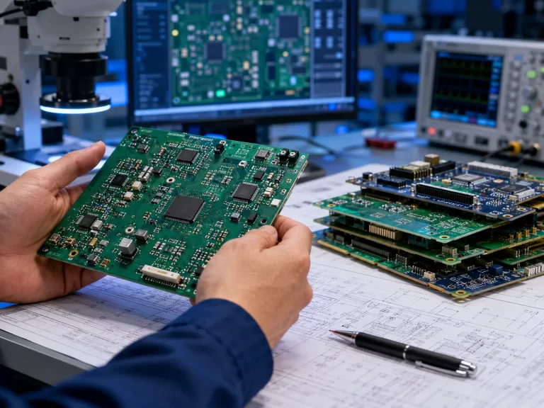
This is the reality behind modern PCB production. End users see a finished board — green solder mask, gold pads, neat silkscreen. But engineers know the truth: the performance of any PCB is determined long before assembly. It is defined during material selection, lamination cycles, copper plating chemistry, drilling precision, and final inspection discipline.
In this in-depth technical report, we break down the complete PCB manufacturing process — not as a textbook overview, but as an engineering-level analysis of what truly determines reliability, scalability, and application success.

The Modern PCB: Why Manufacturing Precision Matters More Than Ever
Today’s electronics operate in harsher environments than ever before:
-
5G RF systems with controlled impedance
-
Automotive ECUs facing vibration and temperature cycling
-
Medical electronics requiring ultra-high reliability
-
Industrial automation running 24/7
A PCB is no longer just a carrier. It is a structural, thermal, and electrical backbone.
Companies like PCB manufacturing experts at jscircuit have invested heavily in advanced fabrication controls to meet these growing requirements. As circuit density increases and tolerances shrink below 75μm line/space, process stability becomes a competitive differentiator.
Research from IPC shows that over 70% of field PCB failures are directly traceable to manufacturing process variation — not design errors. That makes manufacturing excellence mission-critical.
Raw Material Selection: The First Critical Variable
Before a single trace is etched, PCB quality begins with material science.
Core Material
Most rigid PCBs use FR-4 epoxy glass laminate. However, performance depends on:
-
Tg (glass transition temperature)
-
CTE (coefficient of thermal expansion)
-
Dielectric constant stability
-
Resin content uniformity
In high-frequency applications, dielectric stability becomes essential for signal integrity.
For detailed background on structural board types, see Rigid PCB technology overview, where application-specific material strategies are discussed.
Copper Foil Quality
Copper weight and surface treatment impact:
-
Current carrying capacity
-
Thermal dissipation
-
Adhesion strength
-
Fine line etching accuracy
Electrodeposited vs. rolled annealed copper choices can directly affect high-speed designs.
Imaging and Etching: Where Circuit Geometry Is Defined
The imaging stage determines trace accuracy.
Modern PCB fabrication uses:
-
Dry film photoresist lamination
-
Laser direct imaging (LDI)
-
UV exposure
-
Chemical development
LDI systems significantly reduce alignment error compared to traditional phototools.
Etching Chemistry
Etching removes unwanted copper. Uniformity here impacts:
-
Trace width tolerance
-
Edge roughness
-
Impedance control
-
Crosstalk behavior
Excessive etching creates undercutting. Insufficient etching creates short risks. Advanced manufacturers use automated chemistry monitoring systems to maintain consistency.
Drilling and Via Formation: Mechanical vs. Laser Precision
Drilling accuracy determines multilayer connectivity reliability.
Modern PCBs may include:
-
Through-hole vias
-
Blind vias
-
Buried vias
-
Microvias (laser drilled)
Mechanical drilling still dominates for larger vias, but high-density interconnect (HDI) boards require laser drilling down to 75μm or smaller.
Improper drilling parameters can cause:
-
Resin smear
-
Inner layer breakout
-
Misregistration
-
Reduced plating adhesion
Copper Plating: The Foundation of Electrical Reliability
Once holes are drilled, plating forms conductive pathways.
The plating process includes:
-
Desmear
-
Electroless copper deposition
-
Electrolytic copper build-up
Uniform copper thickness is critical. IPC standards recommend minimum barrel thickness for reliability under thermal cycling.
According to industry reliability studies, via barrel cracking accounts for nearly 40% of multilayer PCB failures in high-stress environments.
Process control in plating chemistry, current density distribution, and agitation stability are essential.
For deeper context on board structures and flexibility differences, see FPC vs Rigid PCB – Which One Actually Wins in Modern Electronics?.
Lamination: Where Multilayer Integrity Is Created
Multilayer PCB lamination requires:
-
Controlled pressure
-
Vacuum conditions
-
Precise temperature ramp-up profiles
-
Accurate dwell timing
If lamination pressure is inconsistent:
-
Voids form
-
Delamination risk increases
-
Z-axis expansion issues occur
Advanced PCB manufacturers use automated lamination press monitoring systems with real-time pressure tracking to reduce variability.

Solder Mask and Surface Finish: Protection and Performance
After outer layer processing, solder mask protects copper and prevents shorts.
Key considerations:
-
Mask thickness uniformity
-
Registration accuracy
-
Chemical resistance
Surface finishes vary by application:
-
HASL
-
ENIG
-
OSP
-
Immersion Silver
Each finish affects solderability, shelf life, and signal integrity differently.
Flexible PCB Considerations in Modern Manufacturing
While rigid PCBs dominate many industries, flexible circuits are gaining rapid adoption.
If you’re exploring flex technology fundamentals, review What is Flexible PCB? for material and structural insights.
Flexible PCB manufacturing introduces additional complexities:
-
Polyimide substrate handling
-
Controlled bending radius design
-
Adhesive vs. adhesive-less lamination
-
Coverlay precision
Flex circuits require tighter process discipline due to material sensitivity and dynamic use environments.
Industry Applications: Why Manufacturing Must Match the Use Case
PCB requirements vary drastically across industries.
According to sector studies and production data, the following industries demand increasingly strict PCB tolerances:
-
Automotive electronics
-
Medical devices
-
Aerospace systems
-
Telecommunications infrastructure
-
Industrial robotics
For a broader industry overview, see Top 10 Industries That Use Rigid PCB Technology.
Each industry imposes different standards for:
-
Thermal cycling
-
Vibration resistance
-
Moisture tolerance
-
Signal stability
Manufacturing capability must align with end-use requirements.

Quality Assurance: Where Trust Is Earned
A PCB manufacturer’s real strength lies in its inspection systems.
High-reliability PCB manufacturing includes:
-
Automated Optical Inspection (AOI)
-
X-ray inspection
-
Microsection analysis
-
Flying probe testing
-
Electrical continuity testing
-
Impedance verification
Companies that invest in statistical process control (SPC) typically achieve significantly lower defect rates.
You can learn more about manufacturing philosophy and quality focus through the About Us – jscircuit section, which outlines engineering-led production standards.
Common PCB Manufacturing Pain Points — and How They Are Solved
1. Impedance Variability
Solution: Tight dielectric thickness control and test coupon verification.
2. Via Reliability Issues
Solution: Controlled plating thickness and thermal shock testing.
3. Delamination
Solution: Optimized lamination cycle profiling.
4. Copper Thickness Inconsistency
Solution: Real-time bath chemistry monitoring.
Manufacturers that prioritize these controls reduce warranty risks and long-term lifecycle costs.
Data-Driven Perspective: Why Process Control Matters
Industry reports indicate:
-
PCB scrap rates can exceed 8% without advanced control systems.
-
Implementing automated inspection reduces defect escape rate by over 60%.
-
Laser imaging improves alignment accuracy by up to 25% versus traditional methods.
In competitive markets, these margins determine profitability and reputation.

Frequently Asked Questions
1. What are the main stages of PCB manufacturing?
The main stages include material preparation, imaging, etching, drilling, plating, lamination, solder mask application, surface finishing, and final inspection.
2. What causes PCB failures most often?
Manufacturing variation, especially in plating thickness, lamination pressure, and material inconsistencies, accounts for a majority of field failures.
3. How long does PCB manufacturing typically take?
Standard production cycles range from several days to multiple weeks depending on layer count, complexity, and volume.
4. What is the difference between rigid and flexible PCB manufacturing?
Rigid PCB manufacturing focuses on FR-4 laminates and structural stability, while flexible PCB production requires polyimide materials and bending durability control.
5. How do I choose a reliable PCB manufacturer?
Look for manufacturers with advanced inspection systems, clear process documentation, engineering transparency, and strong industry experience. You can reach out directly via Contact Us – jscircuit for project discussions.
Manufacturing Is the Real Differentiator
Returning to our opening lab scene:
The failed board wasn’t a design failure. It was a process failure.
In today’s electronics landscape, the PCB manufacturing process is not just a production step — it is a reliability engine. Material selection, plating control, lamination precision, and inspection discipline collectively determine long-term success.
As PCBs become thinner, denser, and more application-specific, manufacturing capability becomes strategic infrastructure.
Understanding the PCB manufacturing process is no longer optional for engineers and procurement leaders. It is essential.
And in an industry where microns define outcomes, process excellence defines trust.